PicPort®-Pro-CL-PMCPicPort®-Pro-CL-PMC is a frame grabber supporting the Camera Link standard interface. This high-speed board can be used with both line-scan and area-scan Camera Link compatible cameras. It is suitable for both color and monochrome applications, and supports high-speed and high-resolution. PicPort®-Pro-CL-PMC is cost effective, compact and high performance, meeting the demanding requirements of diverse image processing and machine vision applications. It is a member of the LV Camera Link Family of products. The PMC version of PicPort®-Pro-CL series is compatible with our LVmPC® embedded vision system. Besides the PMC module version, the standard PCI bus version of the PicPort®-Pro-CL series is also available. PicPort®-Pro-CL-PMC main highlights:
|
ArchitectureA comprehensive array of on-board features include Camera Link interface for 1 base camera @ 85 MHz, large LUTs, Bayer color decoder, multi-taps/packed pixel reformatting, color/monochrome format conversion, 32MB 0.7GB/s frame buffer with advanced features and 32/64-bit, 33/66 MHz PCI bus interface with 16 DMA channels. The frame buffer ensures no data loss under varying operating system conditions by virtue of its memory size and its ability to generate interrupts to the user application that flag dynamic image buffer watermark depth thresholds.
PicPort®-Pro-CL-PMC architecture is user friendly, em-ploying innovative re-programmable flash memory and FPGA (Field Programmable Gate Array) technologies. This allows the user to reconfigure the on-board hardware via downloadable software updates. The flash memory can also be used for security coding to prevent unauthorized copying of user application proprietary technology. Image Acquisition & ConditioningCamera Link InterfacesSimultaneously supports 1 base (3 × 8-bit or 2 × 8/10/12-bit or 1 × 8/10/12/14/16-bit monochrome or 24-bit RGB) camera. Area-scan up to 64K × 64K and line-scan up to 64K × infinity with input frequencies up to 85 MHz. Camera Link control lines for asynchronous reset and exposure control. Camera Link serial ports for camera setup and control. General Purpose input/output InterfacesCamera power, LVDS/TTL and opto-coupler input/outputs are accessible via the PCI backplate 6-pin hirose connector or via a 40-pin header socket on the PCB top edge. Camera power is provided for 1 camera and is +5V or +12V selectable. These are available on both Hirose and header connectors. Resettable fuses of 1A are provided for both. LVDS and TTL inputs/outputs share physical pins (GPIO0..2_P, GPIO0..2_N, GPIO3). Selection of direction and standard is via software control. They may be configured as up to 3 LVDS I/O signal pairs (GPIO0..2_P/N) or up to 3 single-nded TTL I/O (GPIO0..2_P). In case of single-ended signals, the negative pin (GPIO0..2_N) cannot be used. GPIO3 is a TTL I/O signal only. Each signal/pair may be selected either as input or as output. The signals are distributed over the two I/O connectors (Basic I/O and Universal I/O connector). 7 opto-coupler inputs and 7 outputs are provided on the header connectors. These have built-in resistors to minimize external components. The opto inputs are independently controllable. The opto outputs are grouped into 2 banks (0..3/4..6), with four (0..3) resp. three (4..6) outputs. The Collector pins (OptoCx) of one bank do have pull-up resistors to a common rail TAP24V_03/46 which must be connected to the desired operation voltage (+5..24V). The Emitter pins (OptoEx) are normally connected to the ground terminal of the external voltage source. More details about the optocoupler interface can be found in the section below. All I/O pins are protected by over/under voltage protection devices clamping to +5V and ground. Application note «External trigger and flash» gives good overview of applications involving external devices such as trigger and flash and about connecting such devices to the frame grabber. LUTs2 LUTs are provided for user configuration as dual 4K × 12 or quad 256 × 8. As the physical memories are organized as 256K × 18, multiple banks are available. Real-Time Function: Bayer DecoderA Bayer color decoder provides high-speed decoding of the Bayer pattern output by many color cameras. Using this on-board facility is an economical and fast solution to this color decoding requirement. Restrictions may appear for multi-tap cameras. Data Storage and TransferFrame BufferA 32MB frame buffer is provided to buffer and re-format the pixel data grabbed from the camera, before passing it to the PCI bus DMA. A sophisticated controller facilitates combining of camera taps into a raster output to the PCI DMA. Features include:
DMA ControllerOutput data from the Frame Buffer is passed to the DMA controller. This innovative design allows up to 16 DMA channels to be user defined, controlling data burst transfers over the PCI bus. Each DMA channel can also define a Region-Of-Interest within the data stream and can also re-transmit the data to multiple destinations on the PCI bus. In conjunction with the color/monochrome data formatter, various formats of the image data can be transferred to host memory or graphic display memory. Host Bus InterfaceA +3.3V compatible PCI bus interface is provided that can operate at 32/64-bit, 33/66MHz. This provides hi-end PCI bus bandwidth at an affordable price. Flash Memory ControllerThe on-board flash memory stores the various configurations of the board that are loaded at power-up and also any software technology security information (software dongle). ConfigurationsPicPort®-Pro-CL-PMC exists in following different fix configurations:
Applications
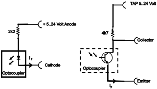
Digital I/O InterfaceGeneral Purpose I/OPicPort®-Pro-CL-Mono-PMC board provides various general purpose input/output interfaces. Location and pinout of the connectors is described section Connector Description. Camera power, LVDS/TTL and opto-coupler input/outputs are accessible via the PCI backplate 6-pin Hirose connector or via a 40-pin header socket on the PCB top edge. Camera power is provided for 1 camera and is +5V or +12V selectable (via on-board jumpers). These are available on both Hirose and header connectors. Resettable fuses are provided for both. LVDS and TTL inputs/outputs share physical pins (GPIO_P0..2, GPIO_N0..2). Selection of direction and standard is via software control. Up to 3 LVDS or TTL pairs are available. Each pair can be selected as 1 LVDS input or 1 LVDS output or 2 TTL inputs or 2 TTL outputs. One pair is on the Hirose connector and two pairs on the header connector. There is also 1 unique TTL input/output on the Hirose connector. 8 optocoupler inputs and 8 outputs are provided on the header connectors. These have built-in resistors to minimize external components. The 8 opto inputs are grouped into 4 pairs (01/23/45/67), each pair having a common Anode (+) and 2 Cathode (-) pins. The 8 opto outputs are grouped into 2 banks (0..3/4..7), each with 4 outputs. The Collector pins (OptoCx) of one bank do have pull-up resistors to a common rail TAP24V_03/47 which must be connected to the desired operation voltage (+5..24V). The Emitter pins (OptoEx) are normally connected to the ground terminal of the external voltage source. More details about the optocoupler interface are provided in the section below. All I/O pins are protected by over/under voltage protection devices clamping to +5V and ground. Optocoupler InterfaceFor use in industrial environment, PicPort®-Pro boards provide I/O signals isolated by use of optocouplers with variable 5V to 24V interface. To take full profit of this signal isolation, you have to connect the optocoupler to an external power supply. The optocoupler input is prepared for input signals from 5 V to 24 V with the appropriate onboard serial resistors. The optooupler output is prepared for external voltage from 5 V to 24 V.
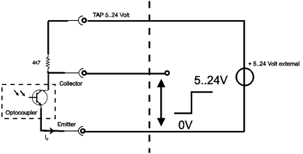
See also the following examples of optocoupler output. In industrial environment, signal levels of 24 V are usually needed.
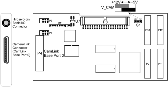
Application note «External trigger and flash» gives good overview of applications involving external devices such as trigger and flash. SoftwareDriver SoftwareLeutron Vision Software Development Suite, LV-SDS, is a software development package (Windows, Linux, VxWorks) that allows full control of all PicPort® and PicProdigy® products. The suite consists of Daisy - the basic software interface for PicPort®/PicProdigy® cards, Camera Editor - easy interactive setup of standard and non-standard cameras, DRAL - a library for handling specific time-critical tasks, Orchid - high level library (DLL or OCX) for quick and easy design of PicPort®/PicProdigy® applications, TWAIN Driver and Video for Windows - provide a simple interface between Leutron Vision hardware and other office and image manipulation programs (e.g. MS Office, CorelDRAW, etc.). The software products come complete with a set of demo programs and additional examples with source code as a guide to the programmer in developing particular applications. To obtain more comprehensive information please download the LV-SDS manual. Third Party SoftwareSeveral well-known third party packages for real-time image processing and analysis are also supported. The packages include HALCON, Activ Vision Tools, NeuroCheck, and others. Please refer to our detailed software brochure (PDF) for more details. Connector Description, Wiring SchemesConnector positionsThis chapter provides description of the connectors, jumpers and DIP switches of PicPort®-Pro-CL-PMC. The following image show locations and pin #1 positions of all the connectors described below.
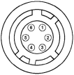
Camera connectorStandard CameraLink connectors for base configuration. Please refer to official CameraLink specification to get the connector pinout. Basic I/O connectorHirose 6-pin female connector with camera power output and general purpose I/O signals; the connector is accessible from the backplate of the board.
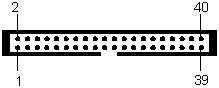
Universal I/O ConnectorMale 40-pin header socket (P8 on figure above) with camera power output, opto-coupler interface, and general purpose I/O; the connector is not directly accessible from the backplate of the board.
Note: The header socket connector may be connected via flat cable to a 37-pin D-sub connector (appearing for example on LVmPC back panel). The following table shows also the relevant pins on that connector.
Power Selector JumperA 3-pin male headers (S1) allowing to select the power output voltage that should be delivered to camera through the I/O connectors (see Basic I/O and Universal I/O connector descriptions above). The table below shows how to select between the +5V and +12V voltages for camera power output.
Control DIP SwitchesThe board possesses a DIP-switch device holding two switches (U7 on the figure above). Function description of the switches is described below. The pin marked as rectangle instead of an ellipse corresponds with OFF position of DIP-switch #1.
PCI Gold Bank Protection (DIP Switch 0) PCI Gold Banks should normally never be changed by the user. The prime function of the PCI Gold Banks is to guarantee a recovery mechanism after a Flash Bank programming cycle for an onboard FPGA has failed due to a system crash or power failure. In these cases the Flash Bank programming cycle can not be repeated without rebooting the system. However, since one or more Flash Banks may now contain corrupted FPGA configuration data it must ensured that these banks are not used for FPGA configuration after the next system reboot. For this purpose DIP switch 0 of the Flash Controller (GoldBootSel) must be set to the 'ON' position. In GoldBoot mode the Flash Controller configures the PCI-FPGA from the Gold PCI Bank but leaves the Video-FPGA and CLP-FPGA idle. The Flash programming cycle can now be repeated. After the Flash programming has been completed successfully the GoldBootSel can be reset and the system must be power-cycled (not soft-reset) before the Flash Bank update takes effect. Technical Specifications
Complementary and Related ProductsSupporting softwareComprehensive set of software tools consisting of video capture libraries and image processing libraries for Windows XP/2000/NT4, Windows Me/98/95 and for Linux. Please check especially the following ones:
Suitable CamerasPlease check the list of suitable cameras (CameraLink models) for use with PicPort®-Pro-CL. The link invokes page showing wide list of different suitable cameras, allowing you to specify more criterions and restrict the list only to the cameras exactly matching your needs. Correspondent cablesAll the necessary cables for connecting a camera to the framegrabber are available. Related Frame Grabbers
LVmPC®LVmPC® is an ultra compact, mobile image processing system for industrial and machine vision, based on standard PC technology and Leutron's frame grabber series. LVmPC® is available in a huge variety of different configurations. Ordering Information
|
|||||||||||||||||||||||||||||||||||||||||||||||||||||||||||||||||||||||||||||||||||||||||||||||||||||||||||||||||||||||||||||||||||||||||||||||||||||||||||||||||||||||||||||||||||||||||||||||||||||||||||||||||||||||||||||||||||||||||||||||||||||||||||||||||||||||||||||||||||||||||||||||||||||||||||
![]()